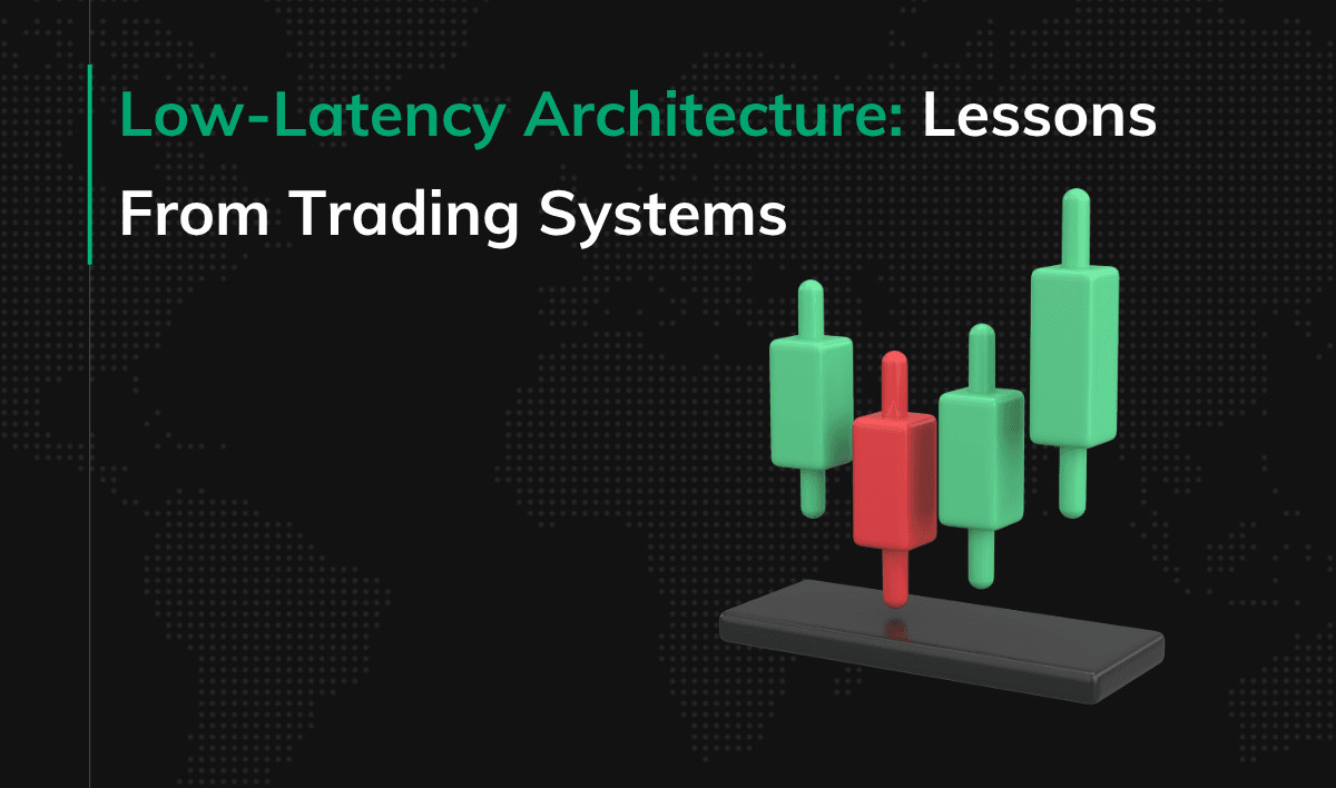
Low-Latency Architecture: Lessons From Trading Systems
Profitability in liquid markets often hangs on the arrival time of a single data packet, and the race to zero latency has pushed system architectures to their physical limits. Because trading infrastructure operates at the extreme edge of physics and computational limits, it serves as a great case study for engineering teams.
While not every application requires nanosecond precision, the solutions pioneered in high-frequency trading provide a blueprint for anyone building performance-critical systems. Observing how trading systems conquer latency reveals valuable insights into architectural trade-offs and deterministic design, helping teams identify bottlenecks and justify when to move logic from software to hardware.
Mapping the journey from tick to trade
The technological limit of modern trading infrastructure is defined by how quickly a system can process market data to reach a decision. While a system may only fire an order for a small fraction of incoming updates, it must evaluate every single “tick” with the same nanosecond precision to ensure it never misses a viable opportunity. Every stage of this evaluation introduces potential delays that can erode the profitability of a strategy.
Defining the transaction window from wire to wire
Wire-to-wire latency provides the most accurate measurement of a system’s total performance. This metric captures the time from the arrival of the first bit of market data at the system’s ingress to the departure of the first bit of an order from the egress port. It is a comprehensive cycle that encompasses physical layer processing, network protocol parsing, order book updates, and the execution of strategy logic alongside regulatory risk checks. Some firms prioritize actionable latency by measuring from the last bit of data received to the first bit of the order sent, but wire-to-wire captures the reality of total data handling from initial receipt to final transmission.
This principle holds true for any latency-sensitive platform: relying on component-level benchmarks often creates a false sense of security. Optimizing an isolated microservice yields little value if the overarching, end-to-end request remains bottlenecked elsewhere in the stack. True system performance is always defined by the full wire-to-wire journey.
Why software-based execution hits a latency wall
Most computing architectures are built for versatility and multitasking, which inherently contradicts the need for singular, deterministic speed. Processing data through a general-purpose processor introduces layers of uncertainty that are difficult to eliminate through optimization alone.
Processor unpredictability and operating system jitter
Operating systems manage multiple tasks by switching between different processes, a method that creates inconsistent delays known as jitter. These systems use interrupts to handle hardware events, forcing the processor to pause trading logic to manage background functions or network traffic. Even when using kernel bypass techniques to streamline data flow, the processor must still move data across the PCIe bus and wait for memory access. These structural bottlenecks and the sequential nature of software execution mean that reaction times can fluctuate significantly depending on the current system load.
For many platforms, this software-induced jitter is an acceptable trade-off for the ease of rapid development and flexibility. However, when business requirements dictate absolute determinism, where missing a microsecond window means losing revenue, the complexity of moving to silicon becomes justified.
Designing for deterministic performance in silicon
The architectural decision to move beyond software is never taken lightly, as hardware development sacrifices flexibility for raw speed. Yet, when a product’s core value proposition relies on unwavering predictability, removing the operating system from the critical path is a necessary business decision. By utilizing FPGAs, engineers replace instruction-based software with direct hardware logic. In this environment, the system does not wait for a processor to fetch and execute a command; instead, the data travels through a pre-configured path of gates designed for one specific purpose.
Processing data in space through hardware logic gates
While a processor handles tasks one by one in a chronological sequence, an FPGA processes them simultaneously in different physical locations on the chip. Trading logic is mapped onto the hardware fabric using look-up tables and flip-flops, essentially turning the strategy into a physical circuit. This spatial layout allows market data parsing, order book updates, and risk checks to happen in parallel rather than competing for the same CPU resources. Because the data flows through a dedicated pipeline of logic gates, there is no risk of a process being delayed by a separate system task.
The precision of hardware clock cycles
Predictability in hardware is a result of everything being tied to a fixed global clock. In a software environment, the time it takes to complete a task can vary based on cache status or system load, but in silicon, every operation is counted in cycles. If a specific logic path is designed to take five clock cycles, the output will appear five cycles later every single time without exception. This creates a level of determinism where jitter is measured in picoseconds rather than microseconds, ensuring that the system reacts with the same speed regardless of how volatile the market becomes.
Controlling the core trading loop on the chip
Moving the trading loop into the silicon gives firms total control over how every bit of data travels through the system. By managing the logic directly on the chip, developers eliminate delays caused by moving data between external components.
Bypassing buffers with high-speed transceivers
High-speed transceivers provide the physical gateway for market data entering the FPGA. Today, it is an industry standard for ultra-low-latency architectures to bypass conventional elastic buffers, which simplify development but introduce additional latency. Streaming data directly into the logic fabric reduces the overhead at the very edge of the hardware, ensuring the data is available for processing the moment it arrives.
Beyond trading, this approach underscores a broader architectural truth. When absolute speed is the goal, standard network buffering becomes a liability. Engineers must aggressively identify and strip away ‘safe’ middleware that stages data, ensuring a direct, unhindered path to the processing logic. Another such example is store-and-forward vs cut-through processing for network data.
Parallel order book management and risk checks
Efficiency in hardware comes from doing many things at once. While software systems typically check risk limits and update order books sequentially, an FPGA handles these tasks in parallel.
| Task | Software Approach | FPGA Approach |
| Order Book | Stored in RAM; prone to cache misses | Stored in on-chip BRAM; 1-cycle access |
| Risk Checks | Sequential (Check A, then Check B) | Parallel (All checks run at once) |
| Data Access | Subject to bus contention | Dedicated, direct logic paths |
By using on-chip memory blocks, the system can access and update the top of the order book in a single clock cycle. Simultaneously, the risk engine evaluates credit limits and order sizes, ensuring that regulatory compliance adds minimal latency to the critical path. Maintaining this level of cycle-accurate precision is the primary goal of hardware-accelerated design.
However, the complexity of managing state and risk in parallel hardware introduces significant development overhead. Because translating software algorithms into physical circuits is a massive undertaking, engineering leaders face a critical trade-off. They must carefully weigh whether the business value of absolute determinism justifies building these systems from scratch, or if leveraging specialized hardware frameworks is a more practical way to bridge the gap between software and silicon.
Optimizing response times with cut-through processing
FPGAs use cut-through processing to react to data before a full packet has even finished arriving. Most systems wait for a message to be fully received to verify the contents, but hardware logic can begin parsing headers immediately. A trading strategy can evaluate a price and prepare an order while the rest of the market data packet is still trailing in through the transceiver. This technique allows the system to send a response the instant the final necessary bit is identified.
The ultimate limit of trading speed
Achieving the fastest possible execution is a balancing act between the physics of transmission and the architecture of the chip. While hardware optimization can reduce the internal logic path to a matter of nanoseconds, the physical medium remains a fixed constraint.
Every meter of fiber optic cable adds almost 5 nanoseconds, just as every Byte of a packet requires 0.8 nanoseconds to be serialized on a 10G line. By embedding state management and trading risk checks directly into hardware, FPGA-based systems operate right at the physical limits of transmission. This specialized architecture ensures that the system is not just fast, but deterministic, providing the consistent performance required to compete in the most sensitive market brackets.
Summary
Trading systems demonstrate what is possible when architecture is optimized ruthlessly for speed. While few industries require the extreme determinism of high-frequency trading, the architectural lessons remain universally applicable. By measuring total wire-to-wire performance, understanding the inherent jitter in operating systems, and knowing when the cost of hardware acceleration is justified, engineering teams can build vastly more efficient and responsive platforms.